In previous posts, we covered taking apart a DasKeyboard, mapping the keys to their corresponding signals on the internal connector, and getting that information neatly cataloged into a MySQL database. In this part of the series, we’ll be looking at how we’re going to map each key to a unique value, or rather a pair of unique values so we can construct a proper lookup table.
If you recall, we have a table in our database that looks like the following:

The key that is a ‘W’ in the qwerty layout represents a comma character in the dvorak layout. The signal combinations for each are laid out in the qwRow, qwCol, dvRow, and dvCol fields. When this key is pressed, it will connect pins 7 and 19. Our programmable logic is going to instead make it look like lines 1 and 21 are connected, thus fooling the host microcontroller into sending a different key code to the host computer.
To do this, we need a series of one bit memories with one memory location for each key. The problem we now need to solve is to figure out how we’re going to create the mapping between the keys and the memory locations.
After giving the problem some thought, I decided that I would assign a unique number to each key. To generate those numbers automatically, I created the following table:
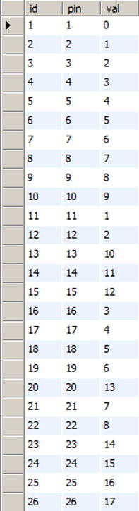
For the moment, ignore the id column (it is a habit of mine to put one in even if redundant). Basically, this table counts upwards as each row or column signal is encountered. Since we know that 11, 12, 16, 17. 18, 19, 21, and 22 are the rows, they count in sequence 1, 2, 3, … ending with 8. The columns do the same, counting from 0 through 17.
This table allows me to use the row and column data to compute a unique memory location for each key. Even better, once you wrap your head around the next bit of sql, you’ll start to see that the database is going to generate our lookup table for us and it will do it in a way that eliminates manual mistakes that might occur if we tried to do it by hand. Here is our query:
select
   (qwC.val * 8) + qwR.val lutAddr,
   (c.val * 8) + r.val tgtLatch
 from keymap k, pinMap c, pinMap r, pinMap qwR, pinMap qwC
 where k.dvCol = c.pin and k.dvRow = r.pin and k.qwCol = qwC.pin and k.qwRow = qwR.pin
order by lutAddr;
The main idea here is that each of our columns contain 8 rows or keys. Because of that, we are going to multiply the column value by 8 and then add the row value to it. This is similar to how you might code a two dimensional array if your language of choice didn’t support two dimensional arrays. The first element would be 1 and the first element of the second column would be 9, and the first element of the third column would be 17 … and so on. Here is a snippet of the results:
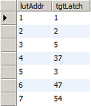
For the first two rows, those keys have no translation going on. They have the same memory address in both layouts. When you get to the key assigned to column1, row 3 (pins 1 and 16) that key then gets translated to be something else. In fact, if you look in the same table, you’ll see that the reverse mapping occurs two rows down. In this particular example, the ‘=’ and ‘]’ keys have swapped locations. The original idea was to use this lookup table to determine where to store the state of each key as it was scanned and then to provide a logical expression that would activate the alternate row/column combinations at the right time in the scan sequence.
If one was very well versed in verilog, I’m sure this implementation would be very easy. Unfortunately, I’m just learning it and am no expert by any means. Instead, I went through the column/row combinations and figured out a process for storing the information and reading it back to the host microcontroller. Once I had a process figured out, writing the code was fairly quick, especially since the database had generated the mappings for me using the above query.
As for the current status of the project, I’ve successfully tested the code on edaplayground.com and it pretty much works as I expected. I then brought the design into the Xilinx ISE, I had a couple of small problems to fix, and then tried to fit the design to a xc2c256 CPLD. It turns out that the CPLD is a nice fit for the project with the code using just a bit over 60% of the devices resources.
I’m getting close to hardware at this point and will hopefully be providing a schematic soon to help demystify some of what I’ve described so far. The code needs some tweaks here and there and that should also be coming soon. The next post will show some rather newbie-ish verilog with some explanation of how we take the table above and turn it into code.
